- 您现在的位置:买卖IC网 > Sheet目录490 > NTMD4184PFR2G (ON Semiconductor)MOSFET P-CH 30V 2.3A 8-SOIC
NTMD4184PF
ELECTRICAL CHARACTERISTICS (T J = 25 ° C unless otherwise noted)
Characteristic
Symbol
Test Condition
Min
Typ
Max
Unit
SCHOTTKY DIODE ELECTRICAL CHARACTERISTICS (T J = 25 ° C unless otherwise noted)
Parameter
Symbol
Test Conditions
Min
Typ
Max
Unit
Maximum Instantaneous
V F
I F = 1.0 A
T J = 25 ° C
0.43
0.50
V
Forward Voltage
I F = 2.0 A
T J = 125 ° C
T J = 25 ° C
T J = 125 ° C
0.35
0.5
0.45
0.39
0.58
0.53
Maximum Instantaneous
I R
V R = 10 V
T J = 25 ° C
0.001
0.02
mA
Reverse Current
V R = 20 V
T J = 125 ° C
T J = 25 ° C
T J = 125 ° C
1.2
0.004
2.0
14
0.05
18
3. Pulse Test: pulse width v 300 m s, duty cycle v 2%.
4. Switching characteristics are independent of operating junction temperatures.
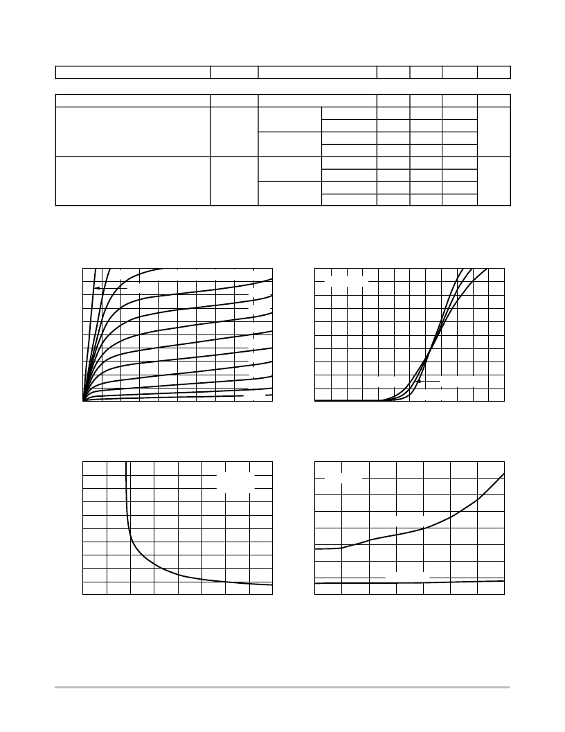
TYPICAL CHARACTERISTICS
10
8
5.0 V
10 V
V GS = 4.5 V
T J = 25 ° C
4.2 V
4.0 V
10
8
V DS ≥ 10 V
3.8 V
6
4
3.6 V
3.4 V
3.2 V
6
4
2
0
3.0 V
2.8 V
2.6 V
2
0
T J = 125 ° C
T J = 25 ° C
T J = -55 ° C
0
2
4
6
8
10
0
1
2
3
4
5
6
0.30
V DS , DRAIN-TO-SOURCE VOLTAGE (V)
Figure 1. On-Region Characteristics
0.25
V GS , GATE-TO-SOURCE VOLTAGE (V)
Figure 2. Transfer Characteristics
0.25
0.20
ID = 3 A
T J = 25 ° C
0.20
0.15
T J = 25 ° C
V GS = 4.5 V
0.15
0.10
0.10
V GS = 10 V
0.05
0.05
2
4
6
8
10
2
3
4
5
6
7
8
9
V GS , GATE-TO-SOURCE VOLTAGE (V)
Figure 3. On-Resistance vs. Gate Voltage
I D , DRAIN CURRENT (A)
Figure 4. On-Resistance vs. Drain Current and
Gate Voltage
http://onsemi.com
3
发布紧急采购,3分钟左右您将得到回复。
相关PDF资料
NTMD4820NR2G
MOSFET N-CH DUAL 30V 4.9A 8-SOIC
NTMD4840NR2G
MOSFET N-CH DUAL 30V 4.5A 8-SOIC
NTMD4884NFR2G
MOSFET N-CH 30V 3.3A 8-SOIC
NTMD5836NLR2G
MOSFET N-CH 40V 11A SO-8FL
NTMD5838NLR2G
MOSFET N-CH 40V 8.9A 8SOIC
NTMD6N02R2
MOSFET PWR N-CH DL 3.92A 20V 8SO
NTMD6N03R2
MOSFET PWR N-CH DL 6A 30V 8SOIC
NTMD6P02R2G
MOSFET PWR P-CHAN DUAL 20V 8SOIC
相关代理商/技术参数
NTMD4820N
制造商:ONSEMI 制造商全称:ON Semiconductor 功能描述:Power MOSFET
NTMD4820NR2G
功能描述:MOSFET NFET SO8 30V 8A TR 0.020R RoHS:否 制造商:STMicroelectronics 晶体管极性:N-Channel 汲极/源极击穿电压:650 V 闸/源击穿电压:25 V 漏极连续电流:130 A 电阻汲极/源极 RDS(导通):0.014 Ohms 配置:Single 最大工作温度: 安装风格:Through Hole 封装 / 箱体:Max247 封装:Tube
NTMD4840N
制造商:ONSEMI 制造商全称:ON Semiconductor 功能描述:Power MOSFET 30 V, 7.5 A, Dual N−Channel, SOIC−8
NTMD4840NR2G
功能描述:MOSFET NFET SO8 30V 7.5A 0.034R RoHS:否 制造商:STMicroelectronics 晶体管极性:N-Channel 汲极/源极击穿电压:650 V 闸/源击穿电压:25 V 漏极连续电流:130 A 电阻汲极/源极 RDS(导通):0.014 Ohms 配置:Single 最大工作温度: 安装风格:Through Hole 封装 / 箱体:Max247 封装:Tube
NTMD4884NF
制造商:ONSEMI 制造商全称:ON Semiconductor 功能描述:Power MOSFET and Schottky Diode
NTMD4884NFR2G
功能描述:MOSFET NFET FTKY S08 30V TR 5.6A RoHS:否 制造商:STMicroelectronics 晶体管极性:N-Channel 汲极/源极击穿电压:650 V 闸/源击穿电压:25 V 漏极连续电流:130 A 电阻汲极/源极 RDS(导通):0.014 Ohms 配置:Single 最大工作温度: 安装风格:Through Hole 封装 / 箱体:Max247 封装:Tube
NTMD4N03
制造商:ONSEMI 制造商全称:ON Semiconductor 功能描述:Power MOSFET 4 A, 30 V, Na??Channel SOa??8 Dual
NTMD4N03R2
功能描述:MOSFET 30V 4A N-Channel RoHS:否 制造商:STMicroelectronics 晶体管极性:N-Channel 汲极/源极击穿电压:650 V 闸/源击穿电压:25 V 漏极连续电流:130 A 电阻汲极/源极 RDS(导通):0.014 Ohms 配置:Single 最大工作温度: 安装风格:Through Hole 封装 / 箱体:Max247 封装:Tube
